WEEK 8
Title of Activities : Circuit Construction 2
Objective : To know how to make PCB layout using ARES 7 Professional (included in Proteus 7)
Activities / Procedures :
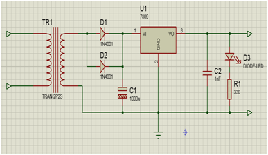
1) This week we are focusing on PCB layout design using ARES 7 Professional. From schematic circuit that we design on Proteus 7, we can automatically transfer it into ARES 7.
2) We can design our own path of copper to connect between one component and another. Copper path need to be tidy and neat to ensure that the line of copper does not touch with one and another(short).
3) PCB layout are provided as below:

PCB LAYOUT WITH TOP
COPPER FOR POWER SUPPLY

PCB LAYOUT WITHOUT
TOP COPPER FOR POWER SUPPLY

PCB LAYOUT WITH TOP
COPPER FOR MICRO CONTROLLER, LCD DISPLAY

PCB LAYOUT WITHOUT TOP
COPPER FOR MICRO CONTROLLER, LCD DISPLAY
Problem encountered :
The problem that we face during designing PCB layout are technically on how to make a good layout based on standard procedure. Width,length,angle and position of component are essential item in designing Pcb layout.
By using Pcb layout software, we can make layout faster instead using manual method that is draw using permanent marker that requires a very skilful hand-drawing.